Researchers at Daegu Gyeongbuk Institute of Science and Technology (DGIST), Ulsan National Institute of Science and Technology (UNIST), and the Institute for Basic Science (IBS) developed a technique to create ultrahigh-definition screens for emerging display technologies. The researchers used the technique, called double-layer dry transfer printing, to build highly efficient LEDs with quantum dots (QLEDs).

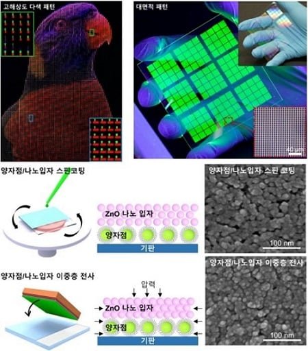
A conceptual diagram of the double-layer dry transfer printing technique. The technique offers high-resolution pixel patterning technology and can be used to create light-emitting devices with ultrahigh-definition and high efficiency for next-generation AR, VR, and wearable displays. Courtesy of DGIST, UNIST, and IBS.
Quantum dots (QDs) offer many advantages as light-emitting materials for displays, including a high photoluminescence quantum yield, wide color range, and high color purity. But the development of a QD patterning process for high-definition pixels and efficient QLEDs is still in the early stages. Conventional dry transfer printing, in which QD ink is applied to a substrate, can be used to make ultrahigh-definition pixels. However, this method has not been used for actual display production, because of its low luminescence efficiency of under 5%.
With the double-layer dry transfer printing technique, the light-emitting and electron-transferring layers of the device can be transferred onto a substrate simultaneously. This reduces interfacial resistance in the device, which facilitates electron injection and the control of leakage charge transport during the fabrication process. By minimizing the leakage current, the external quantum efficiency (EQE) of the QLED devices was increased to 23.3%.
“By using double-layer dry transfer printing technology to reduce interfacial resistance and facilitate electron injection, we have fabricated light-emitting devices that are simultaneously ultrahigh-definition and high efficiency,” professor Ji-woong Yang said. “The light-emitting devices with double-layer thin films fabricated using this technology exhibited high EQE of up to 23.3%, similar to the maximum theoretical efficiency of quantum dot light-emitting devices, which is a very significant result.”
Surface engineering of viscoelastic stamps enabled the researchers to use the double-layer transfer printing technique to create RGB pixelated patterns with 2565 pixels per inch (PPI) and monochromic QD patterns with about 20,526 PPI.
The researchers used the quantum dot/zinc oxide (QD/ZnO) thin film to create ultrahigh-definition patterns of QDs up to 25,526 PPI and achieved an 8 cm x 8 cm area through repeated printing. They demonstrated highly efficient, wearable QLEDs made with the double-layer dry transfer printing technique, confirming the feasibility of using the technique to mass-produce the devices for commercialization.
The double-layer dry transfer printing technique could support the development of full-color QD displays for next-generation display technologies, by providing high-resolution pixel patterning capabilities and creating light-emitting devices with ultrahigh-definition and high efficiency. The technique can be used to produce bright light even with low current.
“We are pleased to have developed a technology that enables higher resolution screens in VR and AR through this research,” professor Moon-kee Choi said. “Through further research, we will strive to broadly apply quantum dots with high color reproduction and color purity to smart wearable devices.”
The research was published in Nature Photonics (www.doi.org/10.1038/s41566-024-01496-x).


